16.11.2020 10:00 CET
Bruno Schuler
EMPA, Switzerland
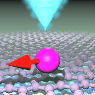
Probing Atomic Quantum Defects in 2D Semiconductors
2D materials are an exciting host to engineer atomic quantum systems by chemical design rules. In this colloquium, I will give an overview on our efforts to design defect systems in monolayer transition metal dichalcogenides (TMDs) by means of chemical doping, Helium ion beam bombardment and atomic manipulation.
We directly resolve the discrete electronic spectrum of single dopants in a charge neutral or ionized state and map out their associated defect orbitals [1-5]. Different types of defects reveal the interplay between chemical impurity states [1-3], multi-valley hydrogenic bound states [4,6], and electron-phonon coupling [1,7] at reduced dimensions. In particular, we will discuss the atomically controlled generation of magnetic carbon radical ions (CRIs) in synthetic TMDs [7] and electrically driven photon emission from individual defects [8].References:
[1] B. Schuler et al., Phys. Rev. Lett. 123, 076801 (2019)
[2] S. Barja et al., Nat. Commun. 10, 3382 (2019)
[3] B. Schuler et al., ACS Nano 13, 10520 (2019)
[4] M. Aghajanian et al., Phys. Rev. B 101, 081201(R) (2020)
[5] E. Mitterreiter et al., Nano Lett. 20, 4437 (2020)
[6] K. Cochrane et al., 2D Mater. 7, 031003 (2020)
[7] K. Cochrane et al., arxiv: 2008.12196
[8] B. Schuler et al., Sci. Adv. 6, eabb5988 (2020)